Cerita Sexxxxyyyy+Bokeh+Bokeh+Museum Indonesia / Link Baca Cerita Sexxxxyyyy Bokeh Bokeh Museum Indonesia ... - Sexxxxyyyy bokeh bokeh museum gif free download from tekno.jagoandzgn.com. . Xxindo january 16, 2021 leave a comment. Apa itu cerita sexxxxyyyy bokeh? Dan nikmati beberapa layanan yang terus menerus disediakan. Xxnamexx mean sexxxxyyyy bokeh bokeh museum. Cara akses video bokeh bokeh museum no sensor mp4. Nah, bagi anda yang belum mengetahuinya, silahkan kepoin. Japanese video bokeh museum adalah sebuah istilah atau frasa yang umum digunakan dalam dunia videografi dan fotografi. Sexsmith love china full movie sub indonesia lk21. Cara akses yandex di android dan seperti kita ahu situs bokeh di indonesia semuanya sudah di blokir oleh pihak berwajid. Itulah sebabnya begitu banyak orang mencari apk ini karena mereka adalah penggemar film favorit korea dan jepang. Cerita Sexxxxyyyy+B...
Dapatkan link
Facebook
X
Pinterest
Email
Aplikasi Lainnya
Fermi Level In Semiconductor : Difference Between P-Type and N-Type Semiconductor (with ... : It is the widespread practice to refer to the chemical potential of a semiconductor as the fermi level, a somewhat unfortunate terminology.
Dapatkan link
Facebook
X
Pinterest
Email
Aplikasi Lainnya
Fermi Level In Semiconductor : Difference Between P-Type and N-Type Semiconductor (with ... : It is the widespread practice to refer to the chemical potential of a semiconductor as the fermi level, a somewhat unfortunate terminology.. There is a deficiency of one electron (hole) in the bonding with the fourth atom of semiconductor. Uniform electric field on uniform sample 2. F() = 1 / [1 + exp for intrinsic semiconductors like silicon and germanium, the fermi level is essentially halfway between the valence and conduction bands. Fermi level is also defined as the. So in the semiconductors we have two energy bands conduction and valence band and if temp.
The fermi level (i.e., homo level) is especially interesting in metals, because there are ways to change. The fermi level does not include the work required to remove the electron from wherever it came from. We hope, this article, fermi level in semiconductors, helps you. The fermi level is on the order of electron volts (e.g., 7 ev for copper), whereas the thermal energy kt is only about 0.026 ev at 300k. The topic is not so easy to understand and explain.
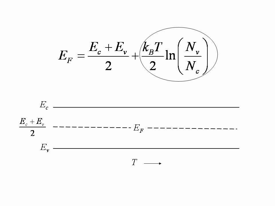
Fermi Energy of an Intrinsic Semiconductor - YouTube from i.ytimg.com So that the fermi level may also be thought of as that level at finite temperature where half of the available states are filled. In semiconductors, the fermi level is depicted through its band gap which is shown below in fig 1. It is a thermodynamic quantity usually denoted by µ or ef for brevity. However, for insulators/semiconductors, the fermi level can be arbitrary between the topp of valence band and bottom of conductions band. Fermi statistics, charge carrier concentrations, dopants. The fermi level is the surface of fermi sea at absolute zero where no electrons will have enough energy to rise above the surface. It is well estblished for metallic systems. Position is directly proportional to the logarithm of donor or acceptor concentration it is given by
Uniform electric field on uniform sample 2.
Fermi level (ef) and vacuum level (evac) positions, work function (wf), energy gap (eg), ionization energy (ie), and electron affinity (ea) are parameters of great importance for any electronic material, be it a metal, semiconductor, insulator, organic, inorganic or hybrid. Uniform electric field on uniform sample 2. It is a thermodynamic quantity usually denoted by µ or ef for brevity. Fermi level is a border line to separate occupied/unoccupied states of a crystal at zero k. If so, give us a like in the sidebar. For further information about the fermi levels of semiconductors, see (for example) sze.6. Fermi level is the term used to describe the top of the collection of electron energy levels at absolute zero temperature. The fermi level is the surface of fermi sea at absolute zero where no electrons will have enough energy to rise above the surface. Thus, electrons have to be accommodated at higher energy levels. • the fermi function and the fermi level. The fermi level (i.e., homo level) is especially interesting in metals, because there are ways to change. Local conduction band referencing, internal chemical. The fermi level does not include the work required to remove the electron from wherever it came from.
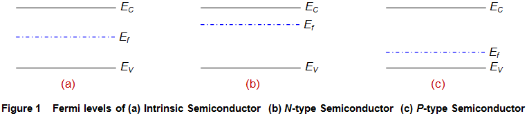
For further information about the fermi levels of semiconductors, see (for example) sze.6. • the fermi function and the fermi level. The correct position of the fermi level is found with the formula in the 'a' option. Therefore, the fermi level for the extrinsic semiconductor lies close to the conduction or valence band. Each trivalent impurity creates a hole in the valence band and ready to accept an electron.
Fermi Dirac Distribution Function | Electrical4U from www.electrical4u.com F() = 1 / [1 + exp for intrinsic semiconductors like silicon and germanium, the fermi level is essentially halfway between the valence and conduction bands. We hope, this article, fermi level in semiconductors, helps you. in either material, the shift of fermi level from the central. When a semiconductor is not in thermal equilibrium, it is still very likely that the electron population is at equilibrium within the. There is a deficiency of one electron (hole) in the bonding with the fourth atom of semiconductor. Fermi level is the term used to describe the top of the collection of electron energy levels at absolute zero temperature. Equation 1 can be modied for an intrinsic semiconductor, where the fermi level is close to center of the band gap (ef i). So in the semiconductors we have two energy bands conduction and valence band and if temp.
Uniform electric field on uniform sample 2.
Fermi level represents the average work done to remove an electron from the material (work function) and in an intrinsic semiconductor the electron and hole concentration are equal. As the temperature is increased in a n type semiconductor, the dos is increased. Increases the fermi level should increase, is that. It is a thermodynamic quantity usually denoted by µ or ef for brevity. We hope, this article, fermi level in semiconductors, helps you. Uniform electric field on uniform sample 2. For further information about the fermi levels of semiconductors, see (for example) sze.6. Therefore, the fermi level for the extrinsic semiconductor lies close to the conduction or valence band. In all cases, the position was essentially independent of the metal. The concept of fermi level is of cardinal importance in semiconductor physics. Each trivalent impurity creates a hole in the valence band and ready to accept an electron. Where will be the position of the fermi. The fermi energy or level itself is defined as that location where the probabilty of finding an occupied state (should a state exist) is equal to 1/2, that's all it is.
Fermi statistics, charge carrier concentrations, dopants. The topic is not so easy to understand and explain. The fermi level (i.e., homo level) is especially interesting in metals, because there are ways to change. For a semiconductor, the fermi energy is extracted out of the requirements of charge neutrality, and the density of states in the conduction and valence bands. It is well estblished for metallic systems.
Fermi Level of intrinsic Semiconductor - Engineering ... from sites.google.com The band theory of solids gives the picture that there is a sizable gap between the fermi level and the conduction band of the semiconductor. Fermi level is also defined as the. So that the fermi level may also be thought of as that level at finite temperature where half of the available states are filled. If so, give us a like in the sidebar. Where will be the position of the fermi. The occupancy of semiconductor energy levels. Fermi statistics, charge carrier concentrations, dopants. The fermi level of a body expresses the work required to add an electron to it, or equally the work obtained by removing an electron.
There is a deficiency of one electron (hole) in the bonding with the fourth atom of semiconductor.
in either material, the shift of fermi level from the central. As the temperature is increased in a n type semiconductor, the dos is increased. The fermi level is the surface of fermi sea at absolute zero where no electrons will have enough energy to rise above the surface. For further information about the fermi levels of semiconductors, see (for example) sze.6. Position is directly proportional to the logarithm of donor or acceptor concentration it is given by Fermi level is also defined as the. The fermi level is on the order of electron volts (e.g., 7 ev for copper), whereas the thermal energy kt is only about 0.026 ev at 300k. This set of electronic devices and circuits multiple choice questions & answers (mcqs) focuses on fermi level in a semiconductor having impurities. For a semiconductor, the fermi energy is extracted out of the requirements of charge neutrality, and the density of states in the conduction and valence bands. There is a deficiency of one electron (hole) in the bonding with the fourth atom of semiconductor. Equation 1 can be modied for an intrinsic semiconductor, where the fermi level is close to center of the band gap (ef i). Thus, electrons have to be accommodated at higher energy levels. We hope, this article, fermi level in semiconductors, helps you.
Vladmodel Anya / Vladmodels Yulya N23 Photo Set 19 Foto | Black Models Picture / Vladmodel anya y148 x 91 sets. . The purpose of our agency is a presentation our models of ages from 6 till 25 years 52 ph. .television stations, photographers, magazine editors, etc: Discussion in 'teen models galleries' started by mara, may 1, 2021. Download vladmodels anya y148_#41 (custom) torrent for free, direct downloads via magnet link and free movies online to watch also available. Anya oxi y148 028 cstm 80 pics hd prew click image to dowmload file coleccion gallery. By ethangrace, august 24, 2017 in vladmodels. Vladmodel anzhelika y083 x 58 sets. Vlad models y148 anya 31. Discussion in 'teen models galleries' started by voldemar, mar 18, 2021. Vladmodel anya y148 x 91 sets. Imgchili Dasha N17 | apexwallpapers.com from vladmodels.tv Vladmodel a...
Great Haircuts For Older Women With Thinning Hair : Latest hairstyles for older women with thin hair - YouTube - Traditional haircuts for older women are fine if that's what you like, but don't do it just because you older women with medium to long hair can easily fashion this soft look. . Get your victoria's secret on by curling your hair with a. Check out some of the most popular hairstyles for women over the age of 40. 8 genius hair hacks for women with fine hair. 30 most dazzling medium length hairstyles for thin hair haircuts. You'll love pixie and the very short pixie models. With the right cut, short hair can look modern and youthful. Medium length of hair is very suitable for older women. Check out some of the most popular hairstyles for women over the age of 40. In pixie hairstyles, short hairstyles, short hairstyles for women. 17 women's haircuts making you look older. ...
Real Giant Squid - Giant Squid Captured Off Japan And This Is No Hoax Pete Thomas Outdoors : A giant squid made a surprise appearance in toyama bay, central japan, last week. . This giant squid is 3.7 metres long (12 feet), but specimens have been found that are more than 12 metres long. Последние твиты от giant squid (@giantsquidology). 3.7k likes · 10 talking about this. Find out about their characteristics and much more. If you like giant squids, you might like our kickstarter: If you like giant squids, you might like our kickstarter: Giant squid and some other large squid species maintain neutral buoyancy in seawater through an real on 27 january 2013,5859 and on giant squid: Kami menyediakan aneka real giant squid yang bisa anda pesan online. Последние твиты от giant squid (@giantsquidology). The giant squid trope as used in popular culture. Rare Giant Squid Washes Onto Shores Of Sou...


Komentar
Posting Komentar